Study on charge-phonon interaction of organic semiconductor towards development of novel electronic property

-
- Principal Investigator
Professor / Hiroyuki YOSHIDA
- Affiliation
Graduate School of Engineering, Chiba University
Researchmap
ORCID ID
- Principal Investigator
Semiconductors play a vital role in powering electrical appliances such as TVs and smartphones. Typical semiconductor materials are silicon, germanium, and gallium arsenide, which are hard and heavy. Therefore, there is a limit to the form of semiconductor products that can be made from these materials. These materials also require a costly manufacturing process that uses a vacuum and high temperature with high energy emissions. In contrast, organic semiconductors are currently attracting attention because of lightweight and flexible. Moreover, its manufacturing cost is very low when the devices are manufactured from the solution process.
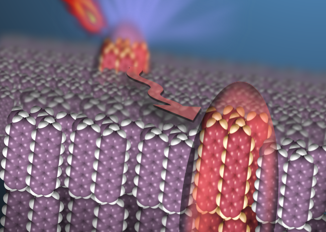
A high-quality flat-panel display using the organic light-emitting diode has already been commercialized for two decades. Further, organic semiconductors can enable unprecedented devices such as thinner than paper solar cells or wearable devices.Since organic substances are generally electrical insulators, organic semiconductors can be considered exceptional in exhibiting electrical conductivity among organic materials. Therefore, the standard theory developed for conventional semiconductors cannot be applied. It is conjectured that charge carriers are transmitted from one molecule to another while deforming the molecules in organic semiconductors. However, the electron and molecular deformation energies are almost similar, making research of charge carrier transport extremely difficult. A breakthrough experimental method that provides critical information about the relation between the charge and molecular deformation is urgently required.
Experimentally obtained band structure (the energy-momentum dispersion relation) gives Yoshida, a Principal Investigator of this project, and his team a fundamental understanding of how the charge carrier conducts in organic materials. They have been developing an experimental technique for this purpose, angle-resolved low-energy inverse photoelectron spectroscopy (AR-LEIPS). For the first time in the world, the team successfully measured the conduction band structure of the organic semiconductor. By analyzing the data, they found that the charge carrier deforms the molecule to form a quasi-particle called polaron. Further, they pursued the effect of polaron formation on the charge transport property, establishing a new model, the partially-dressed polaron. In this project, they will further improve the energy resolution and sensitivity of AR-LEIPS to obtain more detailed information from the band structure. They will then tackle long-standing questions about the charge carrier and molecular deformation. The unraveling of these questions will help them establish a renewed standard theory of the electron conduction mechanism of organic semiconductors. The project's success will enable them to design novel devices that exceed the limits of conventional organic semiconductors. Examples include high-performance thermoelectric conversion elements that generate electricity at human body temperature or transistors and sensors that consume less power. Solar cells and display devices can be mass-produced at a low-cost using printing technology. By combining these techniques, they can create electrical appliances that change the concept of conventional electronic devices, such as lightweight wearable devices that do not require batteries and contribute toward reducing CO2 emissions.


